NZXT Gamma USB 3.0 Casemod
16 Sep 2020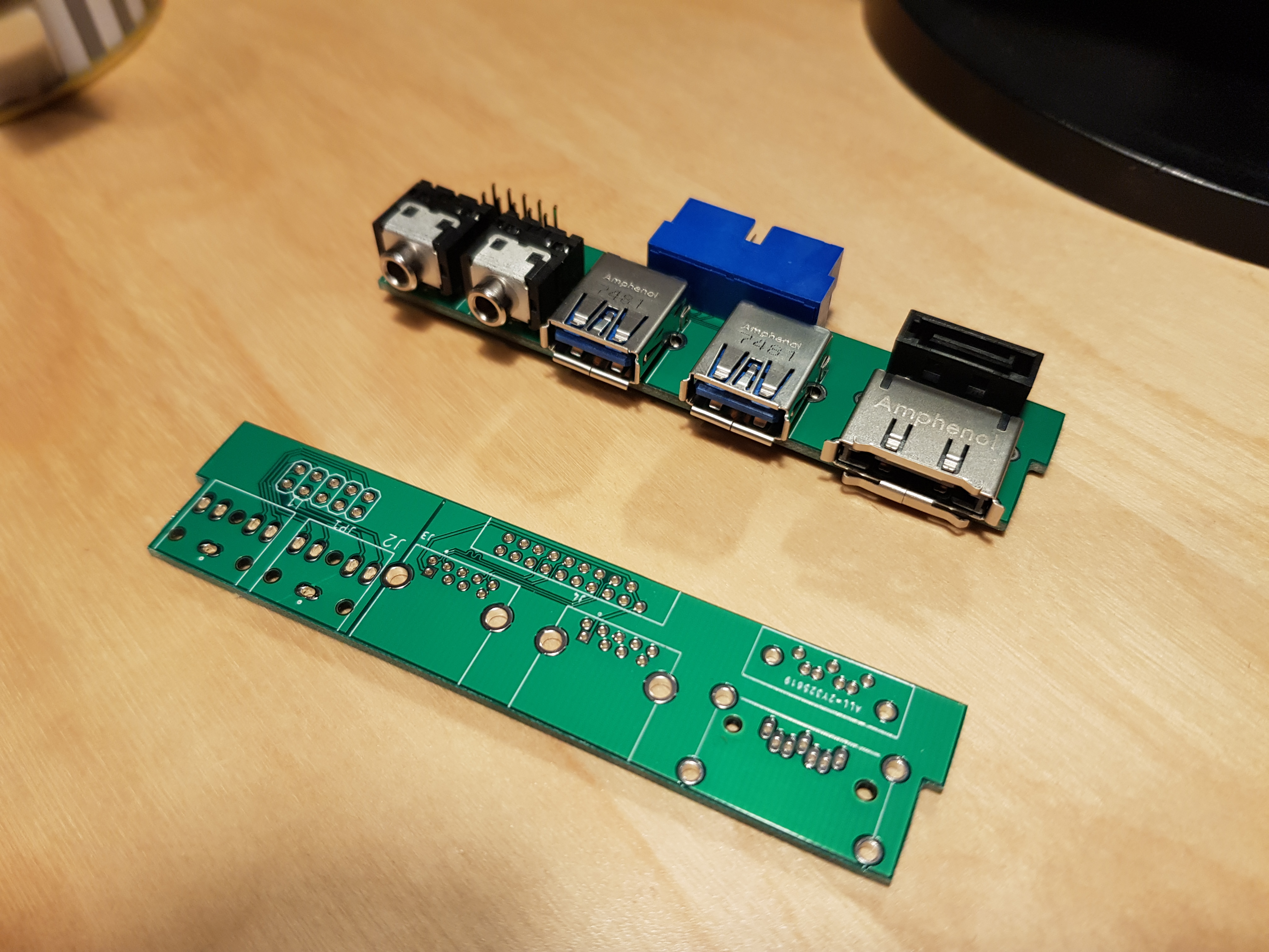
This is a write-up of a project I worked on in 2018 when this blog didn’t exist.
The schematic and board design are available from the Github Project.
Quite a few years ago, I decided to build my own PC; as time marched on I’ve replaced all of the components of the system at least once, except, for the case I originally started with.
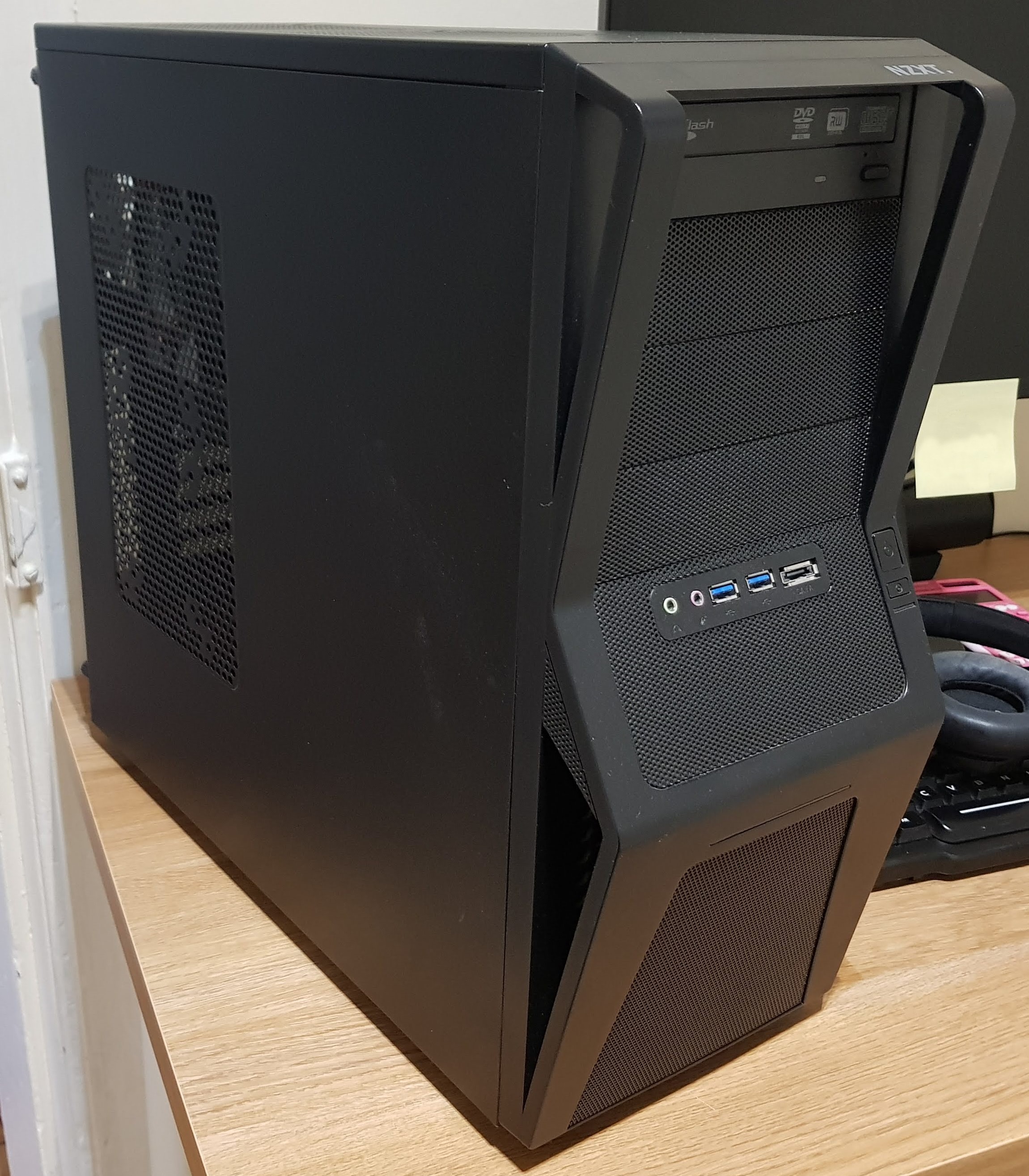
The case is an NZXT Gamma model and in terms in I/O it came with two USB 2.0 ports, your standard 3.5mm audio interfaces and a (doomed) eSATA port. Not exactly the highest-end case at the time, but I had spent all my money on the fun stuff like RAM and a GPU!
 NZXT Gamma Case
Rolling into 2018, I’d just gotten too lazy to reach around the back of my PC to plug in an external hard drive to get those sweet, sweet USB 3.0 speed improvements. So, time to replace those slow, boring, 2.0 ports and bring this case into 2008!
What’re We Working With?
With the advent of USB 3.0, four new pins were added to the port meaning I’d have to replace the front I/O ports with fresh, shiny new USB 3.0 compatible ports.
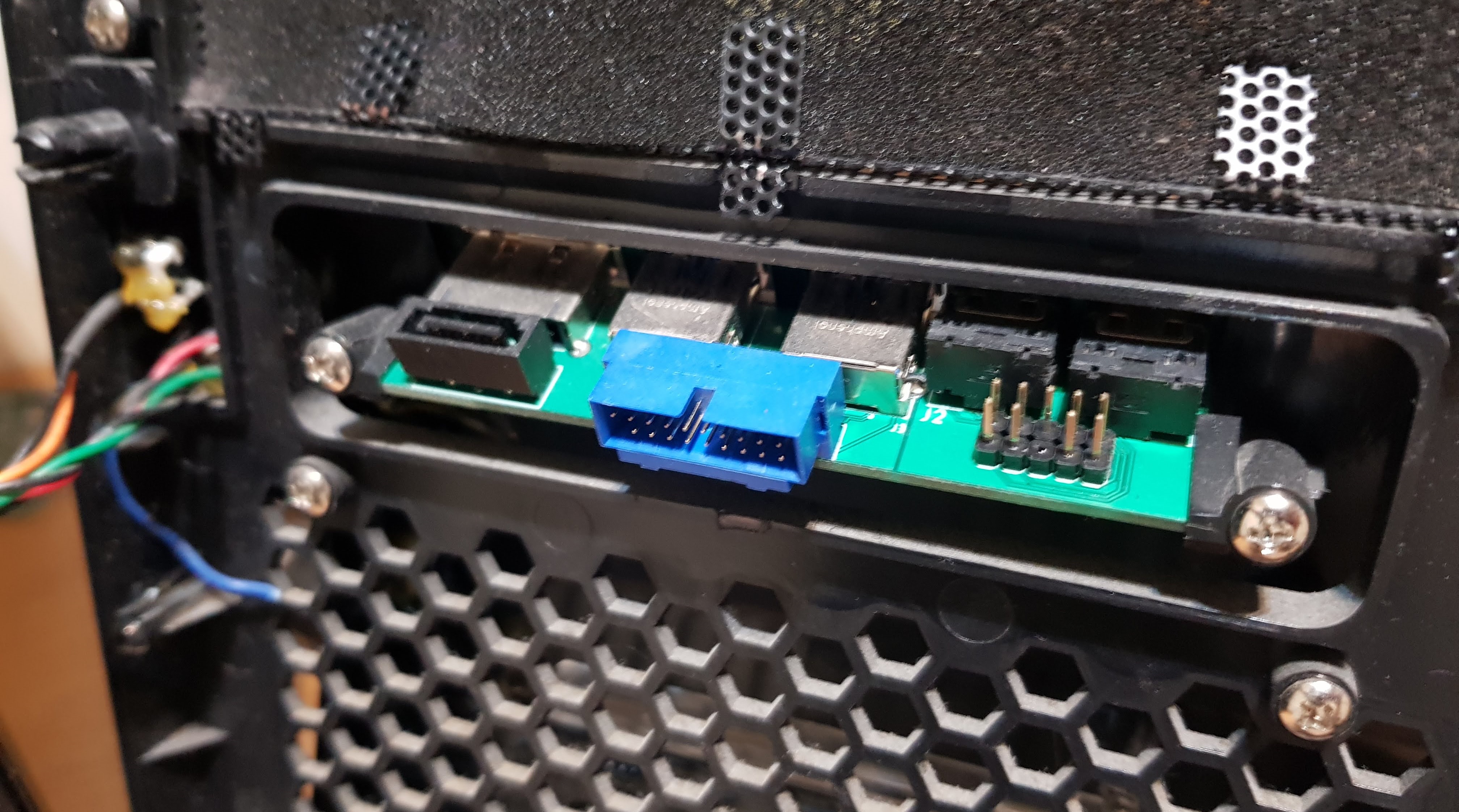
I popped open my case to get a closer look at the front I/O panel and understand how it’s put together so I can plan how to make my high-speed USB dreams a reality. As I expected, all of the I/O ports are mounted to a small PCB which is held in position against the case with a small bracket. This part honestly surprised me as I was expecting the whole thing to be some free floating connectors hot glued into place.
 NZXT Gamma Front-Panel PCB Bracket
I give the NZXT Gamma an “iFixit” repairability score of 9/10 because of this. 👍
Taking a closer look at the board, I can see that it is sensibly laid out, with the audio section and USB/eSATA section clearly mounted to separate ground planes in order to keep the sensitive digital circuitry away from the much more noisy analogue audio section.
Intel HD-Audio
I don’t have any issues with the audio options that came with the case, but if I’m going to replace the USB ports the whole PCB has to go!
In 2004, Intel created the HD Audio Specification that has been a staple of PCs since.
The specification has a lot of features such as support for more channels, higher sampling resolution and rates as well as jack detection, sensing and retasking.
Most of this doesn’t matter, as I’m only implementing a single headphone and microphone channel. However, its worth discussing how exactly the jack detection feature works in HD Audio front panels.
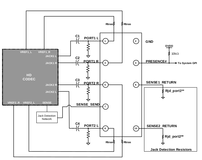
The HD Audio spec does things a little differently when it comes to jack detection compared to other common methods. The specification requires that your jack contains a normally open, isolated switch that is closed when a plug is inserted.
One end of this switch is connected to a resistor network provided on the motherboard and the other side of the switch is connected to a specific resistor value that is also placed on the motherboard to ground.
 Intel® HD Audio Front Panel Analog Header Motherboard Schematic
The CODEC senses that a plug has been inserted when the switch is closed and then can identify exactly which jack was used based on measurements taken of the divider formed.
The reasoning for the somewhat complicated technique is a consideration for the number of sensing pins that would need to be present to support more complicated audio setups such as 7.1 surround systems. CODEC manufacturers would be forced to adopt larger IC packages, which cost more and would, therefore, drive up costs.
The resistor sensing network technique is fairly cheap to implement in silicon and so is a good tradeoff for enabling this kind of feature.
Unfortunately, those Normally Open Isolated Switch type of 3.5mm jacks are almost impossible to find. CUI Inc made the original jacks that came with the case but after trawling their website, the closed matching model is the SJ1-354X series; which doesn’t come in an isolated switch option.
Additionally, the coloured ring surrounding the jack is not an option for any of the products on their website. What I’m looking for is either obsolete or was a custom job for NZXT. Yay
Looks like I’m breaking out the solder sucker and doing some salvage work.
USB 3.0
I’m not going to write a lot about USB 3.0 here, as for this project I’m really only interested in one minor facet of the physical layer, the ports, signal routing and cabling.
So, briefly, lets talk about USB ports; originally, USB Type-A ports had 4 pins.
A VBUS pin, which provides 5V for a connected peripheral, two differential D-
and D+ pins and finally a GND pin.
This worked fine for many years, but there is an issue with only having a single differential pair between a host and peripheral, only one device can use the pair at a time (or Half-Duplex to be technical).
Additionally, the bit-rate for USB 2.0 is limited to a theoretical maximum of 0.48 Gigabit per second.
USB 3.0 solves these problems by adding a transmit and receive differential pair to the physical layer and increases the maximum bit-rate to 5 Gbps!
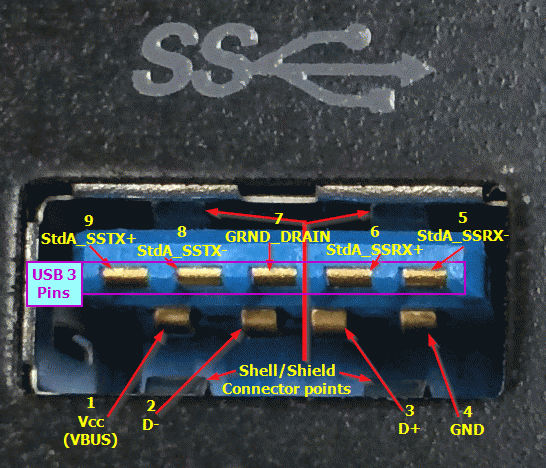 USB 3 Pins Static, Unconventional2, CC BY-SA 4.0
eSATA
There is a port on the original I/O board that implements the eSATA interface, intended for interfacing with external hard drives.
Essentially, this was an interface that was dead on arrival to the market and never got widespread adoption because it never really made sense considering USB 3.0 was available at around the same time and the actual USB interface was not the limiting factor when it came to reading and writing to hard disks (the disks themselves are too slow).
eSATA also doesn’t provide power over the cable, meaning you need to plug an additional USB cable into your HDD anyway.
I think thats enough that needs to be said about eSATA.
The Actual Design
Time for the fun stuff, designing the board.
Starting things off, I used a vernier to find the dimensions of the original interface board so I can simply replace the whole thing in one fell swoop. With an exact copy of the board outline I can simply slot the new board into the bracket with no modification to the case plastics.
Finding the exact position on where to place the audio, USB and eSATA ports was a bit more complicated and involved taking a few different measurement of the ports in relation to the board edges and checking the mechanical drawings of the connectors until everything looked just right.
Firing up EAGLE, I set up a board outline based on my measurements and a simple 2-layer stackup to reflect the original PCB. I also created ground pours on both layers, including the separate analogue and digital planes present on the original PCB.
With all the connectors present on my PCB, routing was a pretty simple task, with exception of USB 3.0 of course.
In the case of USB 3.0, each data signal pair has to be routed together and with as close to the same length as possible and should be no greater than 0.127mm (5 mils). This was pretty easy to achieve with EAGLE’s Meander tool which let me add the necessary extra length to one side of the pair to achieve as close a match as possible.
Additionally, each pair has to be routed with a 90 Ohm differential transmission line, actually working out the spacing and trace width needed to achieve the characteristic impedance target is a bit out of scope but could be a good blog post in the future(Todo list++).
Apart from this bit of extra complexity, this is obviously a very simple but super useful board!
After running my DRC, triple checking my footprints and layouts it’s time to generate some Gerbers and fabricate my board. A few weeks later and my bare PCB has arrived from my low-cost Chinese PCB fab of choice and ready to move onto assembly.
After managing to recover the audio jacks from the original PCB I quickly assembled the new design and threw it into my PC!
The Moment of Truth
Running a smoke-test (turning it on with my hand on the power switch), I observed no magic smoke leakages and decided to move onto real testing.
Plugging my set of sacrificial headphones into the jack my PC quickly switched audio outputs and behaved exactly as I would expect a headphone port to work. There wasn’t anything particularly interesting testing to do beyond this so time to move on to the more interesting business of checking that USB still works!
Using a USB 3.0 Flash drive, I did a few 100 MiB Sequential/Random Read and Write benchmarks using CrystalDiskMark with the original 2.0 ports, the ports on the rear of my motherboard and my shiny, new, USB 3.0 front panel ports.
From this very pretty graph, its obvious that USB 3.0 is much faster than 2.0 in this test and that there was no observable speed difference between the front panel USB ports and the integrated back panel USB ports.
Based on that, I’d call this a success.
I didn’t test eSATA because I never actually set it up on my PC before and have never used it since. But something needed to fill the gap in the case!